Whether you know it or not, VCSELs, or vertical-cavity surface-emitting lasers, have become a key component in everyday life. They work behind the scenes in many applications, including in high-speed optical interconnects in datacenters that enable the flow of internet traffic and in modern cell phones in facial recognition sensing technologies.
Next-generation automotive, aerospace, defense, and industrial applications are requiring solutions with ultra-wide temperature range VCSEL components to enable high-speed optical interconnects in environments that may span a temperature range of -55°C to +125°C (-67°F to +257°F). This is much greater than a typical consumer application or datacenter (0°C to +70°C or +85°C) environment. VCSELs are increasingly being designed into medical, automotive and consumer electronics devices for sensing and facial recognition.
So, what exactly is a VCSEL?
The Anatomy of a VCSEL
VCSEL is the acronym for vertical-cavity surface-emitting laser, which is really just a description of how the device is structured. As the name states, the laser emits from the top surface of the device and offers a very compact laser source with a circular-shaped emission pattern. This makes for easy coupling into an optical fiber and convenient assembly for sensing applications. Figure 1 illustrates the light emission patterns of a light-emitting diode (LED), VCSEL, and edge-emitting laser (EEL). The middle diagram shows the small, circular shape of the VCSEL emission that allows for high-efficiency, low-cost coupling into a standard multimode fiber and directed emission sensing.
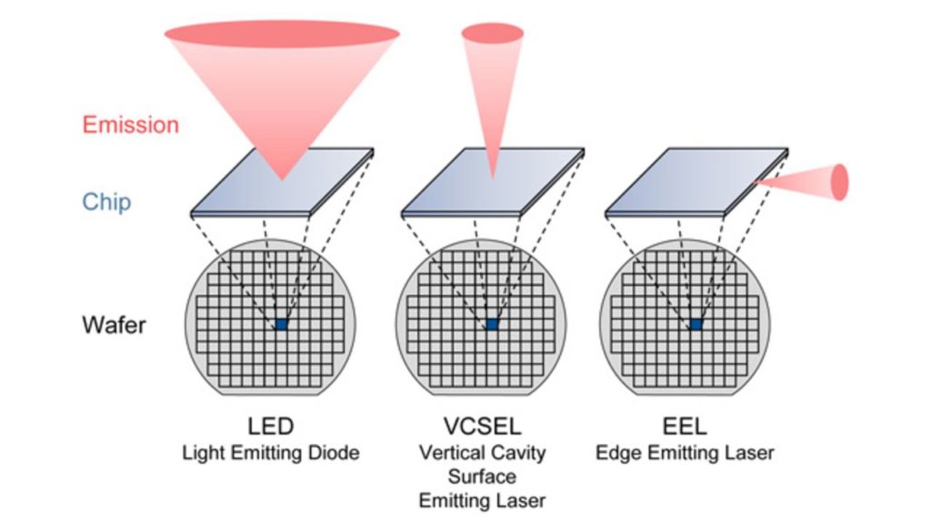
Figure 1 – Emission patterns of an LED, VCSEL, and EEL, illustrating the small circular pattern of the VCSEL that enables easy fiber coupling. (Image from Instrument Systems)
A VCSEL is a laser fabricated from semiconductor materials, which means that the layers of material that make up the laser cavity must lie vertically. The vertical emission is achieved by creating the laser structure in thin epitaxial layers built up on a substrate, almost like the layers of a sandwich. For high reliability, these layers of materials, of which there may be hundreds, must all be extremely high quality with few defects. The epitaxial structure includes mirrors on both sides of the laser cavity so that the light can resonate within the cavity for the laser to have the opportunity to achieve stimulated emission of a single or small group of modes.
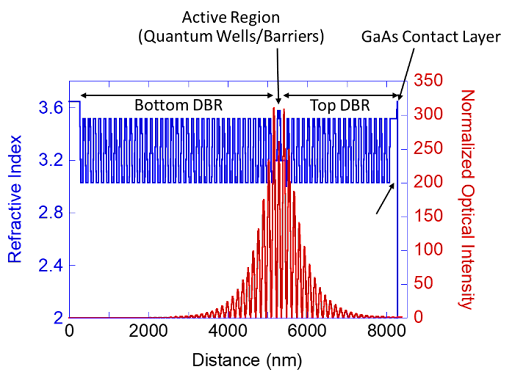
In the VCSEL epitaxy, the mirrors are created with distributed Bragg reflectors (DBRs). The DBRs are made by growing thin 1/4 –wavelength thickness alternating layers of materials that have distinctly different indices of refraction, which then reflect light of that specific wavelength, increasing the optical intensity in the active region, as shown in Figure 2. This is a key component of a VCSEL because it concentrates the light in the active region so that lasing can occur. The anode and cathode contacts must also run through these mirrors, so they are generally doped, or intentionally given specific impurities, to improve electrical conductivity. This is done particularly in the layers further from the cavity, as doping close to the cavity increases optical loss.
Figure 2 – Layers in a typical VCSEL epitaxy structure and optical intensity of the VCSEL structure
The cavity region is the second-most critical component of the VCSEL epitaxial layer structure. It is where the carrier confinement and the optical gain can occur in order to achieve stimulated optical emission. The cavity region consists of strained quantum wells where the gain occurs as well as barrier regions and additional carrier confinement layers to maximize the lasing efficiency, as illustrated in the schematic diagram in Figure 3. It is the details of these quantum well regions that lead to the lasing output light, though also creates some of the most significant challenges in moving to wide-temperature range VCSELs.
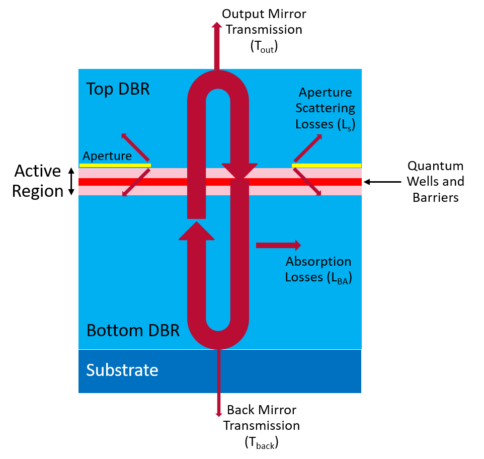
Figure 3 – Schematic of key elements of a VCSEL
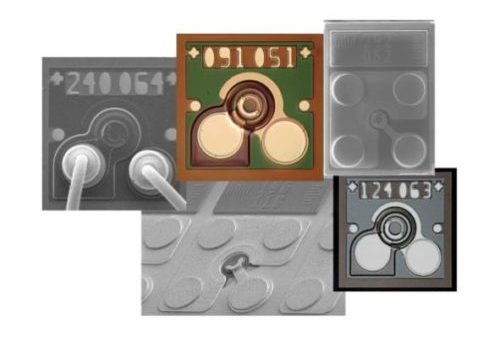
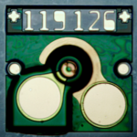
Once the epitaxial structure is grown on a wafer, the wafer must be fabricated through semiconductor processing to create the individual VCSEL devices, of which there are tens to hundreds of thousands of devices on each wafer. During this fabrication process, individual mesas are etched and an oxidation process is performed to get additional current confinement in the lateral directions. Passivation layers are added and metals are deposited to create the anode and cathode contacts, resulting in a 3D device, a general sample of which is shown in Figure 4. Finally, the wafer must undergo lapping and dicing to create the thin, tiny individual VCSEL devices.
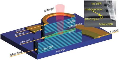
Figure 4 – 3D model of a VCSEL (Image from SPTS)
Wide Temperature VCSEL Performance Characteristics
What changes for a wide temperature range VCSEL? Typical datacenter applications have focused on ensuring sufficient optical output power with lower bias currents at higher temperatures because that is where the worst-case operating point was for those environments. Legacy standards based on the state of VCSEL development 20-30 years ago dictate that most datacenter interconnects use 850nm VCSELs. There was seldom any need for a datacenter VCSEL to operate below 0°C, and definitely not -40°C or -55°C. However, industrial, aerospace, defense, and automotive applications definitely see these types of cold temperatures in addition to very hot temperatures, potentially even up to 125°C. These applications also require highly reliable VCSEL components to pass their rigorous qualification tests.
A wide temperature range VCSEL must have excellent optical output laser power across the full range of operation, reasonable drive currents, and high reliability over a temperature range of 165°C or even 180°C to be an effective component in the system. In order to meet these requirements, the alignment of the cavity’s reflectance peak and the optical gain curve must be aligned so that the gain is greater than the losses over the full operating temperature range. These losses increase with temperature, so for VCSEL operation in general, the overall gain decreases with temperature.
But it’s not quite as simple as that because the VCSEL design can also be adjusted to shift the cavity peak, so if more gain is required at higher temperature, the curves can be shifted. But shift that curve too much toward the higher temperatures, and the gain may fall to nearly zero at the cold temperatures. So, there is a definite tradeoff in the design of VCSELs for wide temperature operation!
VCSELs supporting -55°C to +125°C for the ultra-wide temperature range of applications seen in aerospace, automotive, industrial, and defense applications will be extremely important in the next generation of high-speed optical interconnects. Design modifications and even different wavelength VCSELs will be required to meet the rigorous environmental and reliability requirements of these applications. Higher wavelengths, such as 940nm and 980nm VCSELs, have higher gain, are showing excellent performance characteristics, and outstanding reliability across the full temperature range and are beginning to see market traction in transceiver applications due to their improved performance characteristics. VCSELs may be just a tiny component, but they have become a part of everyday life in more ways than we know!